Phasics
- Wavefront, MTF and QPI measurement solutions
- Products
- Applications
- Markets
- Company
- Contact us

June 12, 2026
From 193 nm ArF projection lenses to 405 nm maskless writers, UV and deep-UV optical systems cover multiple wavelengths, numerical aperture ranges, source conditions and imaging architectures. A 193 nm immersion scanner, a 248 nm KrF tool, a 365 nm i-line stepper, a 375/405 nm maskless writer and a 266 nm inspection or microfabrication setup do not impose the same metrology constraints.
This is why wavefront characterization in UV and DUV systems cannot be reduced to a one-size-fits-all measurement. The relevant measurement approach depends not only on the operating wavelength, NA range, optical path and source configuration, but also on what needs to be characterized: the optical component itself, the beam delivered by the source, or the complete beam-plus-optics system under real operating conditions.
From diffraction-limited resolution to an engineering problem
Lithography systems are projection imaging systems whose resolving capability is often summarized by the Rayleigh formula:
CD = k1 * λ / NA
where CD is the critical dimension, λ is the exposure wavelength, NA is the numerical aperture of the projection optics and k1 is a process factor. In lithography, k1 reflects the combined contribution of illumination strategy, mask technology, optical proximity correction, photoresist response and downstream process optimization. ASML notes that the physical limit for k1 is approximately 0.25⁽¹⁾.
This scaling relationship shows that reducing CD depends mainly on three levers: shortening the exposure wavelength, increasing the projection lens NA, and lowering the effective k1 through illumination optimization, resolution enhancement techniques and computational lithography. ASML also describes how off-axis illumination and pupil shaping can be used to improve imaging performance by controlling how light interacts with the mask pattern.
However, once a process moves toward shorter wavelengths, higher NA and lower k1 values, the optical system has far less tolerance for residual error. Residual wavefront aberration, field-dependent wavefront error, thermally induced wavefront drift and illumination pupil imbalance can all modify the aerial image at the wafer plane. The consequences include reduced image contrast, lower image log-slope, compressed depth of focus and a narrower exposure-dose process window. DUV lithography studies have used metrics such as depth of focus, mask error enhancement factor and image log-slope to quantify these effects ⁽²⁾.
Wavefront quality is therefore a link between projection lens performance, aerial image fidelity, CD control and process-window stability. For high-NA DUV imaging systems, high-sensitivity wavefront measurement at the operating wavelength, across relevant field points and under realistic thermal conditions is not a refinement. It is part of the engineering basis for repeatable imaging.
Why wavefront, not only MTF or CD?
MTF and CD-based evaluations describe system response or printed outcome. Wavefront data adds a diagnostic and process-control layer, enabling engineers to monitor the optical system throughout manufacturing, assembly and alignment rather than testing only the final result.
By decomposing the measured wavefront into defocus, astigmatism, coma, spherical aberration and higher-order terms, engineers can identify where an imaging limitation comes from and use that information to guide correction steps.
This distinction is important in UV and DUV systems because the same loss of imaging performance may result from different physical causes: lens alignment, thermal drift, field-dependent aberration, source instability, coating behavior or test-architecture limitations. Wavefront metrology helps connect the observable performance change to a correctable optical origin.
UV and DUV systems span different wavelengths and architectures
193 nm ArF: immersion and dry projection optics
In advanced front-end manufacturing, 193 nm ArF immersion lithography has long been used for demanding patterning steps. The ASML TWINSCAN NXT:2050i ⁽³⁾ is a representative high-end immersion ArF scanner, with a 1.35 NA projection lens for 300 mm wafer volume production. Here, the NA refers to the effective wafer-side numerical aperture in the immersion medium, not an equivalent NA in air.
Even as EUV is used for selected critical layers at leading nodes, 193 nm immersion remains relevant for many complementary patterning steps. In such production environments, DUV and EUV tools must be considered together, particularly for overlay and cross-matching. ASML describes the TWINSCAN NXT:2100i, the successor to the NXT:2050i, as incorporating improvements for DUV-EUV cross-matching overlay.
Dry ArF systems remain an important engineering reference for 193 nm projection optics. For dry ArF lithography and high-NA DUV optical modules, NA around 0.93 represents a representative high-end practical condition in air. The ASML TWINSCAN XT:1460K ⁽⁴⁾ contains a variable 0.65-0.93 NA 193 nm projection lens, which illustrates the optical requirements of this architecture.
At these NA levels, the engineering focus extends beyond nominal resolution. Residual wavefront error, field-dependent aberration, thermally induced drift and slit-position consistency all influence aerial image stability. High-sensitivity wavefront characterization is therefore relevant to projection lens design validation, objective alignment, thermal behavior analysis and process-related aberration control.
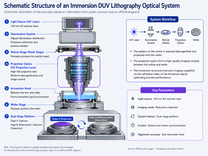
Figure 1. Structure of a DUV immersion lithography system
248 nm KrF: projection optics for mature and specialty processes
248 nm KrF lithography remains important for mature nodes and specialty process flows. KrF projection systems commonly operate in dry configurations with NAs ranging from moderate values to high-NA systems. Nikon’s NSR-S220D⁽⁵⁾, for example, uses a 248 nm KrF excimer laser, a 0.82 NA projection lens, a 1:4 reduction ratio and a 26 mm x 33 mm maximum exposure field.
For more demanding KrF applications, ASML identifies the TWINSCAN XT:1060K as its most advanced KrF system. ASML public materials have described it as a 0.93 NA KrF system for more critical KrF layers.
Increasing NA improves resolution but also reduces depth of focus approximately with 1/NA². In mature-node or non-critical-layer applications, the most relevant optical trade-off may therefore not be the highest possible resolution. It may instead be the balance between resolution, DOF, overlay, field uniformity and process robustness.
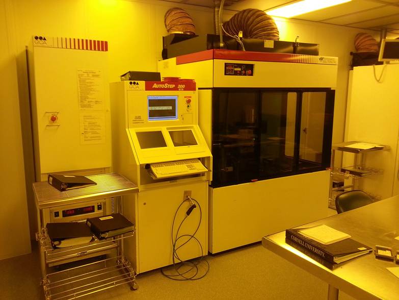
Figure 2. Example of an i-line stepper lithography system.
Image credit: a13ean, Wikimedia Commons, CC BY-SA 3.0.
365 nm i-line: a wider application space than the roadmap suggests
365 nm i-line systems cover more than one architecture and use case. High-resolution i-line steppers, such as the Canon FPA-3030i5+ ⁽⁶⁾ with variable NA from 0.45 to 0.63, target sub-micron lithography at 365 nm. [8] ASML’s TWINSCAN XT:400L contains a variable 0.65 NA 365 nm projection lens and is specified for production resolutions down to 350 nm, 280 nm with annular illumination, and 220 nm with annular illumination plus a high-resolution option.
The i-line ecosystem also includes contact, proximity and lower-NA projection systems used for MEMS, thick resist, packaging-related substrates and non-flat wafers. In these cases, the metrology focus often shifts from ultimate resolution toward depth of focus, substrate tolerance, focal-plane stability, distortion control, overlay behavior and field uniformity.
For such systems, wavefront and system-level characterization need to reflect the process target. A low-NA thick-resist process and a high-resolution i-line stepper do not require the same test architecture, even though they operate at the same nominal wavelength.
375 nm and 405 nm: maskless direct-write systems
At 375 nm and 405 nm, maskless direct-write systems often use digital pattern writing rather than reticle-based projection exposure. Heidelberg Instruments’ MLA 150, for example, can be configured with 375 nm and/or 405 nm laser wavelengths and uses a maskless alignment architecture for sub-micron patterning.
These systems are used in applications such as MEMS, micro-optics, microfluidics, prototyping and packaging-related development. Their optical evaluation is usually closer to system-level performance validation than to classical high-NA projection lens qualification. Alignment accuracy, field uniformity, stitching behavior, focus stability and substrate adaptability may be more important than aberration-limited resolution alone.
266 nm: inspection, laser processing and specialty DUV optics
The 266 nm band, typically generated as the fourth harmonic of Nd:YAG lasers, is used in several specialized DUV applications. In photomask manufacturing, KLA describes TeraScan as using DUV image acquisition for pre- and post-pellicle pattern inspection and incoming quality control. In laser processing, 266 nm is also used for precision microfabrication, thin-film processing, laser repair and interference or direct-write patterning.
These applications require flexible metrology configurations. The relevant measurement may target a component, a laser processing objective, a reflective or catadioptric module, a beam-conditioning path, or a complete inspection subsystem.
Four dimensions of a UV/DUV wavefront measurement approach
1. Wavelength match
Measuring at a wavelength different from the design wavelength can introduce coating-response differences, material dispersion and refractive-index offsets. For a 193 nm optical system, a measurement performed at 633 nm may not represent the same optical path. The closer the test wavelength is to the operating wavelength, the more directly the wavefront data can be interpreted for engineering decisions.
2. NA coverage
At high NA, the pupil edge can carry process-relevant aberration information. A measurement configuration that cannot sample the full pupil, or that loses accuracy at the periphery, may miss exactly the region that matters for image contrast, DOF and CD stability. Dynamic range, spatial sampling density and compatibility with strongly converging or diverging beams are therefore central requirements.
3. Source conditions
UV and DUV sources are not neutral elements in the measurement chain. Spectral linewidth, pulse-to-pulse stability, beam quality and thermal load can all affect the measured wavefront over time. In many cases, a single static acquisition is not sufficient. Repeated measurements, thermal drift analysis and dynamic monitoring provide a more representative view of the system behavior.
4. Test architecture and project stage
The most appropriate measurement architecture depends on the stage of the project. R&D work may require flexibility, sample comparison and aberration decomposition. Assembly and alignment require real-time feedback, repeatability and sensitivity to adjustment. System-level validation requires stability data, multi-field-point consistency and results that can be correlated with imaging or process metrics.
Phasics measurement platforms for UV and DUV optical systems
Phasics wavefront sensors are based on quadriwave lateral shearing interferometry (QWLSI), a self-referencing technique that uses a two-dimensional diffraction grating to generate laterally sheared replicas of the incoming wavefront on a detector. The recorded interferogram encodes the wavefront gradient across the aperture in a single acquisition, without a separate external reference beam. This architecture supports compact and mechanically stable measurement configurations, which is valuable in UV test environments.
For UV and deep-UV applications, Phasics provides wavefront sensors, modular platforms (Kaleo Kit) and custom integration solutions that can be configured according to the operating wavelength, NA condition, source configuration and optical architecture of the system under test.
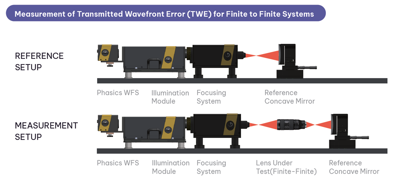
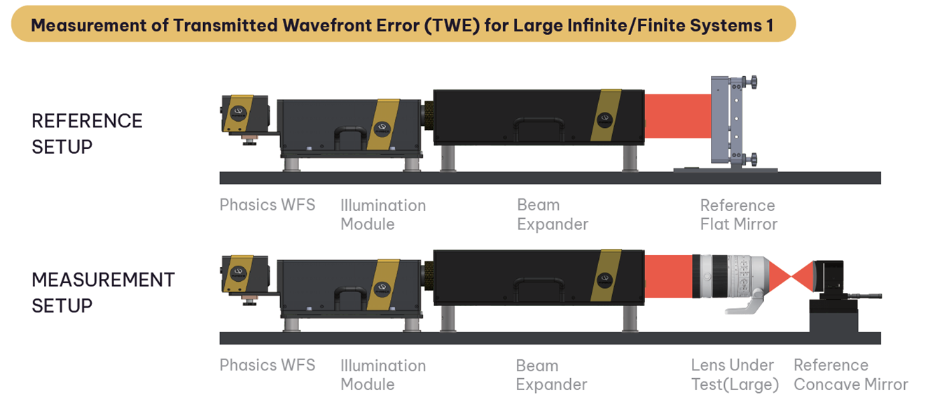
Figure 3. Phasics UV objective measurement setup. Top: finite-to-finite system. Bottom: infinite-to-finite system.
SID4-UV / SID4-UV HR
For the UV spectral range, SID4-UV / SID4-UV HR wavefront sensors are designed for measurements from 190 nm to 400 nm. The SID4-UV HR product page specifies 512 x 512 measurement points and 2 nm RMS (λ /133 RMS at 266 nm) sensitivity in the ultraviolet spectrum, making it suitable for optical component characterization and UV/DUV Wavefront metrology test benches .
Typical use cases include UV/DUV optical component characterization, UV source quality control, objective and module testing, and integration into dedicated metrology benches.
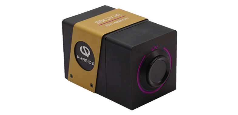
Figure 4. SID4-UV wavefront sensor.
Kaleo Kit modular platform and custom integration
Beyond standalone wavefront sensors, Phasics can provide modular UV/DUV test platforms and pre-integrated solutions. Depending on the project, a Kaleo Kit configuration can combine the wavefront sensor, source selection or source integration, beam conditioning optics, reference components and analysis software.
For customers that do not yet have a suitable DUV source, the platform can be configured with an integrated source when feasible. For customers that already have a 193 nm, 248 nm, 266 nm or other UV/DUV source, Phasics can evaluate integration feasibility and design a metrology architecture matched to the source parameters, interface constraints and measurement objectives.
Where the project requires high-NA DUV measurement, Kaleo Kit can be configured with appropriate reference optics and beam-conditioning modules. Depending on the configuration, it can support TWE/RWE measurement, Zernike aberration decomposition, multi-field-point comparison and stability analysis, with measurement configurations up to approximately NA 0.95.
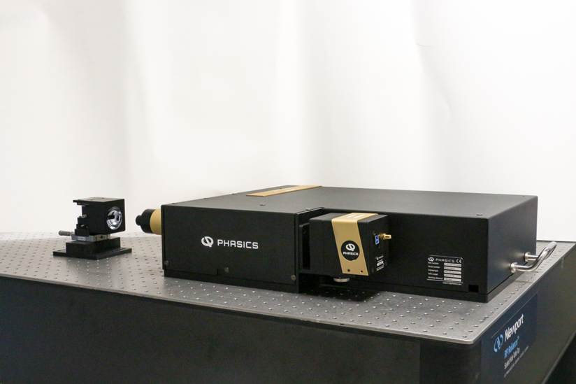
Figure 5. Phasics 266 nm DUV Kaleo Kit wavefront measurement platform.
From optical specification to engineering data
The central question in UV and DUV optical metrology is not only whether an optical system meets a specification. It is whether the measurement reveals why the system behaves as it does under realistic operating conditions.
A 193 nm ArF projection objective, a 248 nm KrF system, a 365 nm i-line stepper, a 375/405 nm maskless writer and a 266 nm inspection or microfabrication setup all belong to the broader UV optical metrology landscape, but their characterization priorities are not the same. The appropriate wavefront measurement method must therefore be built around the wavelength, NA range, source condition, test architecture and engineering phase of the system.
By combining wavefront maps, Zernike decomposition, TWE/RWE analysis, multi-field-point comparison and stability monitoring, engineering teams can turn optical performance into actionable data for design validation, alignment optimization, thermal drift analysis and system-level qualification.
Discuss your application
If you are working on a UV or DUV optical system, from 193 nm ArF to 405 nm maskless direct writing, Phasics can help evaluate the most appropriate wavefront measurement approach for your wavelength, NA range and test architecture.
References
[1] ASML, The Rayleigh criterion, Lithography Principles.
[2] Zhang S. et al., Applied Optics, 61(20), 6023–6032 (2022). DOI: 10.1364/AO.462436
[3] ASML, duv-lithography-systems, twinscan-nxt2050i
[4] ASML,duv-lithography-systems, twinscan-xt1460k
[5] Nikon, Semiconductor Lithography Systems Lineup: NSR-S220D.
[6] Canon, FPA-3030i5+
Wang X. et al., Materials Today, 67, 299–319 (2023). DOI: 10.1016/j.mattod.2023.05.027